GaN HEMT Models 101: How Do Nonlinear Models Help with GaN PA Design?
May 31, 2018
 This
is the first blog in a series explaining the basics of model-based PA
design.
Gallium nitride (GaN) power amplifier (PA) design is a hot topic these days. For many reasons, GaN HEMT devices have emerged as the leading solution for most new microwave PA needs.
Traditionally, PA design has been done with approximate starting points and lots of “guru” knowledge. Using measured load-pull data can enhance PA design success, but it may not be available at the desired application frequencies. Instead, you can use accurate nonlinear models to generate design data faster, target more precise PA behavior and achieve better results.
In this blog post, we’ll cover the basics you need to know for
nonlinear GaN models. If you already know them, jump straight to Part 2, which
explains the fundamentals of I-V curves.
What’s a nonlinear GaN model?
For many engineers, the first step in designing a PA is going to the data sheet for a transistor product and viewing the S-parameters. An S-parameter file is useful, but it doesn’t give enough information about the large-signal operation of the device. Additionally, PA design engineers can use measured load-pull data to find optimal load impedance targets for optimal power and efficiency at specified frequencies.
However, using load-pull data with a simulation model allows a designer to do much more. Specifically, with a properly extracted nonlinear model, designers can:
- Find optimal load and source impedance targets for optimizing any linear or nonlinear performance goal. This can be done quickly at any frequency within the model’s valid frequency range.
- Simulate the maximum limits of operation.
- Balance a PA designer’s challenging linearity, power, bandwidth and efficiency goals.
- Speed up the design process and help get the design right the first time.
- Lower product development costs.
Over the past few years, Modelithics has collaborated closely with Qorvo to develop an extensive library of nonlinear models that now represents more than 70 die and packaged Qorvo GaN transistors. These models allow PA designers to accurately predict the performance of the transistor when integrated into their schematic. Modelithics’ simulation models integrate seamlessly with the latest electronic design automation (EDA) simulation tools, including National Instruments' NI AWR Design Environment and Keysight Technologies’ Advanced Design System (ADS). You can learn more and request free access to the Modelithics Qorvo GaN Library at https://www.modelithics.com/mvp/qorvo.
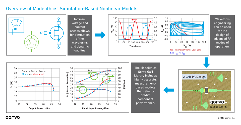
The image below shows how simulations are used to create a PA design. Qorvo and Modelithics use select models to generate PA reference designs. We then fabricate, test and document these designs to illustrate the model’s accuracy and usefulness for design application, as well as the capabilities of the individual GaN device at the PA circuit level.
Learn More: Device and PA Circuit Level Validations of a High Power GaN Model Library
Modelithics Qorvo GaN Library
Our library contains high-accuracy nonlinear simulation models for Qorvo GaN transistor devices.

Modelithics’ nonlinear GaN models have design features including
variable bias, temperature scaling, self-heating effects, intrinsic
current-voltage (I-V) sensing, and bond wire settings when applicable.
Capturing the I-V curve
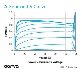
At its most basic level, a nonlinear GaN model has to capture the current-voltage characteristic curve, or I-V curve, of the transistor at different levels of operation. The I-V characteristic of a transistor dictates the primary power, efficiency and other key performance drivers of a device.
We go into I-V curves in more depth in Part 2 of this blog series, but in essence, an I-V curve is a graph of drain-to-source current (I) versus drain-to-source voltage (V), parameterized for varied gate-to-source voltages. The voltage limit on the high end is set by the breakdown voltage, and the current limit is set by the maximum current. See the following figure for a generic I-V curve.
To be useful for PA design, properly extracted models must capture the boundaries of these I-V curves, along with the many other aspects that are required to properly represent DC and dynamic RF behavior at both small- and large-signal operation.
Learn More: Model-Based GaN
PA Design Basics: What’s in an I-V Curve?

What’s in a model?
A model’s ability to predict the nonlinear behavior of a PA transistor is based on several key aspects:
- The representation of the voltage-dependent current source (Ids)
- Voltage-dependent capacitances (primarily gate-to-source Cgd and drain-to-source Cgs)
- Voltage-dependent diode models, which are related to the prediction of breakdown voltage
- Parasitic inductance, capacitance and resistance to represent the overall frequency-dependent behavior of the device
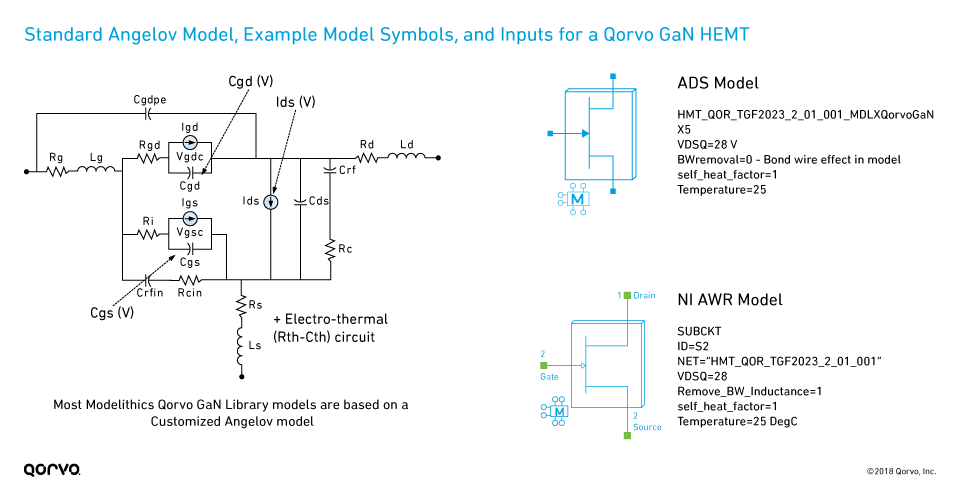
The baseline used in the Modelithics Qorvo GaN Library is a customized model
based on the Chalmers-Angelov model. The
following figure shows the basic model topology, which, like small-signal
models, contains all the elements needed to fit the S-parameter data over
frequency. This modeling framework can also be used to fit noise parameters for low-noise and high-power applications.
Learn More: Advanced Nonlinear and Noise Modeling of High Frequency GaN Devices

The previous figure also shows several typical symbols that you can see in Modelithics Qorvo GaN models:
- Temperature: The ambient temperature for the device’s operation.
- BWremoval: A bond wire de-embed switch.
- self_heat_factor: This input enables the model to estimate variability in self heating of, for example, a pulsed signal versus a continuous wave (CW) signal input. This input is set to the duty cycle of the pulsed signal.
- VDSQ: Some models have a VdsQ input that allows you to scale the intended operating voltage (e.g., over a range of 12 V to 28 V), which can be thought of as a scalable model sweet spot.
You can also find the features for an individual Modelithics model in the
model’s information data sheet, which is available by double-clicking on
the model within the simulator and then clicking on the Help (ADS) or Vendor Help (AWR) button.
The importance of heat in GaN designs
GaN is one of the most popular PA transistor technologies because of three key properties:
- High breakdown field (which is related to high breakdown voltage)
- High saturation velocity (related to high maximum current, Imax)
- Outstanding thermal properties
Learn More: A Primer on GaN
and 3 Reasons It Outperforms Other Semiconductors in RF Applications
Download GaN For Dummies®
Learn about the basic technology of GaN and its applications in RF design.
But there’s a consequence to achieving a higher power capability:
- Higher power means higher DC power.
- Any applied DC power that isn’t converted to RF output power will be dissipated as heat (unless the efficiency of the transistor is 100%).
As a result, GaN transistors get very hot thermally, and thermal management
becomes an important design consideration. Fortunately, GaN on silicon carbide
(GaN on SiC) is better able to handle the heat, with its high thermal
conductivity of 5 W-cm-1K-1 (compared to 1
W-cm-1K-1 for silicon).
But at the PA circuit level, this means designers have to consider thermals
along with all their other design challenges — and GaN models can help.
From a modeling point of view, all Modelithics Qorvo GaN models have both
ambient temperature and self-heating effects built into the models. Some
models also have channel temperature sensing nodes to allow designers to
monitor estimated channel temperature during the RF design phase.
Next up: What’s in an I-V curve?
Now that you've learned some of the basics about Modelithics' nonlinear GaN models, read Part 2 for a deeper dive on how to read and understand I‑V curves and how they can help your GaN PA design process.
Have another topic that you would like Qorvo experts to cover? Email your suggestions to the Qorvo Blog team and it could be featured in an upcoming post. Please include your contact information in the body of the email.

